
January 10, 2017
Semiconductor eyed for next-generation ‘power electronics’
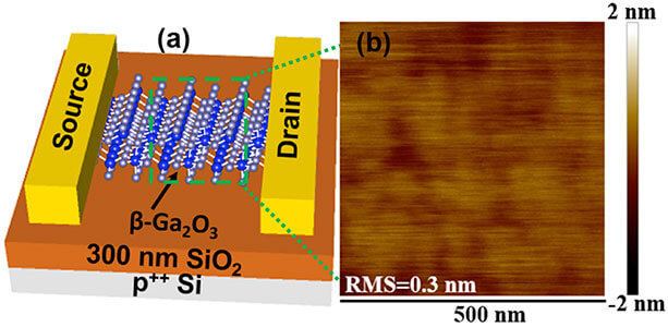 The schematic at left shows the design for an experimental transistor made of a semiconductor called beta gallium oxide, which could bring new ultra-efficient switches for applications such as the power grid, military ships and aircraft. At right is an atomic force microscope image of the semiconductor. (Purdue University image/Peide Ye)
Download image
The schematic at left shows the design for an experimental transistor made of a semiconductor called beta gallium oxide, which could bring new ultra-efficient switches for applications such as the power grid, military ships and aircraft. At right is an atomic force microscope image of the semiconductor. (Purdue University image/Peide Ye)
Download image
WEST LAFAYETTE, Ind. – Researchers have demonstrated the high-performance potential of an experimental transistor made of a semiconductor called beta gallium oxide, which could bring new ultra-efficient switches for applications such as the power grid, military ships and aircraft.
The semiconductor is promising for next-generation “power electronics,” or devices needed to control the flow of electrical energy in circuits. Such a technology could help to reduce global energy use and greenhouse gas emissions by replacing less efficient and bulky power electronics switches now in use.
The transistor, called a gallium oxide on insulator field effect transistor, or GOOI, is especially promising because it possesses an “ultra-wide bandgap,” a trait needed for switches in high-voltage applications.
Compared to other semiconductors thought to be promising for the transistors, devices made from beta gallium oxide have a higher “breakdown voltage,” or the voltage at which the device fails, said Peide Ye, Purdue University's Richard J. and Mary Jo Schwartz Professor of Electrical and Computer Engineering.
Findings are detailed in a research paper published this month in IEEE Electron Device Letters. Graduate student Hong Zhou performed much of the research.
The team also developed a new low-cost method using adhesive tape to peel off layers of the semiconductor from a single crystal, representing a far less expensive alternative to a laboratory technique called epitaxy. The market price for a 1-centimeter-by-1.5-centimeter piece of beta gallium oxide produced using epitaxy is about $6,000. In comparison, the “Scotch-tape” approach costs pennies and it can be used to cut films of the beta gallium oxide material into belts or “nano-membranes,” which can then be transferred to a conventional silicon disc and manufactured into devices, Ye said.
The technique was found to yield extremely smooth films, having a surface roughness of 0.3 nanometers, which is another factor that bodes well for its use in electronic devices, said Ye, who is affiliated with the NEPTUNE Center for Power and Energy Research, funded by the U.S. Office of Naval Research and based at Purdue’s Discovery Park. Related research was supported by the center.
The Purdue team achieved electrical currents 10 to 100 times greater than other research groups working with the semiconductor, Ye said.
One drawback to the material is that it possesses poor thermal properties. To help solve the problem, future research may include work to attach the material to a substrate of diamond or aluminum nitride.
The research was based at Discovery Park’s Birck Nanotechnology Center.
Writer: Emil Venere, 765-494-4709, venere@purdue.edu
Source: Peide Ye, 765-494-7611, yep@purdue.edu
Note to Journalists: A copy of the research paper is available from Emil Venere, Purdue News Service, at 765-494-4709, venere@purdue.edu
ABSTRACT
High Performance Depletion/Enhancement-Mode β-Ga2O3 on Insulator (GOOI) Field-effect Transistors with Record Drain Currents of 600/450 mA/mm
Hong Zhou, Mengwei Si, Sami Alghmadi, Gang Qiu, Lingming Yang, Peide D. Ye, Fellow, IEEE
School of Electrical and Computer Engineering and Birck Nanotechnology Center, Purdue University, West Lafayette, IN, 47907 USA (e-mail: yep@purdue.edu)
In this letter, we report on high performance depletion/enhancement (D/E)-mode β-Ga2O3 on insulator (GOOI) field-effect transistors (FETs) with record high drain currents (ID) of 600/450 mA/mm, which are nearly one order of magnitude higher than any other reported ID values. The threshold voltage (VT) can be modulated by varying the thickness of the β-Ga2O3 films and the E-mode GOOI FET can be simply achieved by shrinking the β-Ga2O3 film thickness. Benefiting from the good interface between β-Ga2O3 and SiO2 and wide bandgap of β-Ga2O3, a negligible transfer characteristic hysteresis, high ID on/off ratio of 1010, and low subthreshold swing of 140 mV/dec for a 300 nm thick SiO2 are observed. E-mode GOOI FET with source to drain spacing of 0.9 μm demonstrates a breakdown voltage of 185 V and an average electric field (E) of 2 MV/cm, showing the great promise of GOOI FET for future power devices.
