
April 12, 2017
Graphene ‘phototransistor’ promising for optical technologies
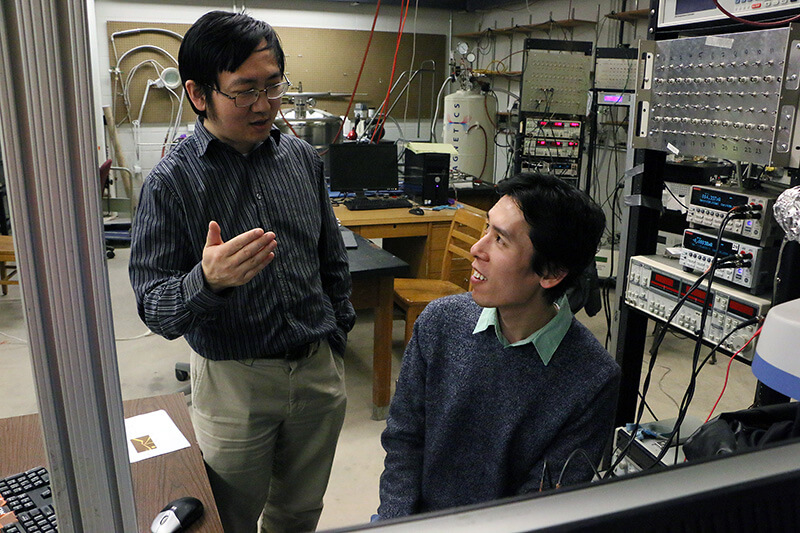
Yong Chen, at left, a Purdue University professor of physics and astronomy and electrical and computer engineering, and graduate student Ting-Fung Chung discuss their research to develop highly sensitive optical devices made of a material called graphene. The advance could help bring applications from imaging and displays to sensors and high-speed communications. (Purdue University image/Erin Easterling)
WEST LAFAYETTE, Ind. – Researchers have solved a problem hindering development of highly sensitive optical devices made of a material called graphene, an advance that could bring applications from imaging and displays to sensors and high-speed communications.
Graphene is an extremely thin layer of carbon that is promising for optoelectronics, and researchers are trying to develop graphene-based photodetectors, devices that are critical for many technologies. However, typical photodetectors made of graphene have only a small area that is sensitive to light, limiting their performance.
Now, researchers have solved the problem by combining graphene with a comparatively much larger silicon carbide substrate, creating graphene field-effect transistors, or GFETs, which can be activated by light, said Yong Chen, a Purdue University professor of physics and astronomy and electrical and computer engineering, and director of the Purdue Quantum Center.
High-performance photodetectors might be useful for applications including high-speed communications and ultra-sensitive cameras for astrophysics, as well as sensing applications and wearable electronics. Arrays of the graphene-based transistors might bring high-resolution imaging and displays.
“In most cameras you need lots of pixels,” said Igor Jovanovic, a professor of nuclear engineering and radiological sciences at the University of Michigan. “However, our approach could make possible a very sensitive camera where you have relatively few pixels but still have high resolution.”
New findings are detailed in a research paper appearing this week in the journal Nature Nanotechnology. The work was performed by researchers at Purdue, the University of Michigan and Pennsylvania State University. A YouTube video is available at https://youtu.be/wKvoechAq6U.
“In typical graphene-based photodetectors demonstrated so far, the photoresponse only comes from specific locations near graphene over an area much smaller than the device size,” Jovanovic said. “However, for many optoelectronic device applications, it is desirable to obtain photoresponse and positional sensitivity over a much larger area.”
New findings show the device is responsive to light even when the silicon carbide is illuminated at distances far from the graphene. The performance can be increased by as much as 10 times depending on which part of the material is illuminated. The new phototransistor also is “position-sensitive,” meaning it can determine the location from which the light is coming, which is important for imaging applications and for detectors.
“This is the first time anyone has demonstrated the use of a small piece of graphene on a large wafer of silicon carbide to achieve non-local photodetection, so the light doesn’t have to hit the graphene itself,” Chen said. “Here, the light can be incident on a much larger area, almost a millimeter, which has not been done before.”
A voltage is applied between the back side of the silicon carbide and the graphene, setting up an electric field in the silicon carbide. Incoming light generates “photo carriers” in the silicon carbide.
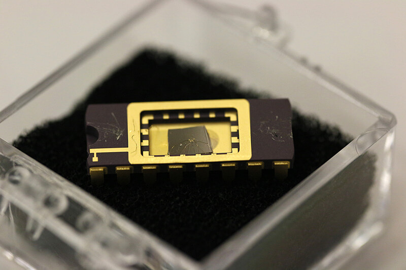 A graphene field-effect transistor, or GFET, developed at Purdue University could bring high-performance photodetectors for various potential applications. (Purdue University image/Erin Easterling)
Download image
A graphene field-effect transistor, or GFET, developed at Purdue University could bring high-performance photodetectors for various potential applications. (Purdue University image/Erin Easterling)
Download image
“The semiconductor provides the media that interact with light,” Jovanovic said. “When light comes in, part of the device becomes conducting and that changes the electric field acting on graphene.”
This change in the electric field also changes the conductivity of graphene itself, which is detected. The approach is called field-effect photo detection.
The silicon carbide is “un-doped,” unlike conventional semiconductors in silicon-based transistors. Being un-doped makes the material an insulator unless it is exposed to light, which temporarily causes it to become partially conductive, changing the electric field on the graphene.
“This is a novelty of this work,” Chen said.
The research is related to work to develop new graphene-based sensors designed to detect radiation and was funded with a joint grant from the National Science Foundation and the U.S. Department of Homeland Security and another grant from the Defense Threat Reduction Agency.
“This particular paper is about a sensor to detect photons, but the principles are the same for other types of radiation,” Chen said. “We are using the sensitive graphene transistor to detect the changed electric field caused by photons, light in this case, interacting with a silicon carbide substrate.”
Light detectors can be used in devices called scintillators, which are used to detect radiation. Ionizing radiation creates brief flashes of light, which in scintillators are detected by devices called photo multiplier tubes, a roughly century-old technology.
“So there is a lot of interest in developing advanced semiconductor-based devices that can achieve the same function,” Jovanovic said.
The paper was authored by former Purdue postdoctoral research associate Biddut K. Sarker; former Penn State graduate student Edward Cazalas; Purdue graduate student Ting-Fung Chung; former Purdue graduate student Isaac Childres; Jovanovic; and Chen.
The researchers also explained their findings with a computational model. The transistors were fabricated at the Birck Nanotechnology Center in Purdue’s Discovery Park.
Future research will include work to explore applications such as scintillators, imaging technologies for astrophysics and sensors for high-energy radiation.
Writer: Emil Venere, 765-494-4709, venere@purdue.edu
Sources: Yong Chen, 765-494-0947, chen276@purdue.edu
Igor Jovanovic, 734-647-4989, ijov@umich.edu
Note to Journalists: A copy of the research paper is available from Emil Venere, Purdue News Service, at 765-494-4709, venere@purdue.edu, or by contacting the Nature Press Office at press@nature.com. A YouTube video is available at https://youtu.be/wKvoechAq6U. Other multimedia materials are available on Google Drive at https://goo.gl/0vRakO. The materials were prepared by Erin Easterling, digital producer for the Purdue College of Engineering, 765-496-3388, easterling@purdue.edu.
ABSTRACT
Position dependent and millimeter-range photodetection in phototransistors with micron-scale graphene on SiC
Biddut K. Sarker,1,2 † Edward Cazalas,3† Ting-Fung Chung,1,2† Isaac Childres,1,2 Igor Jovanovic,3, 4 and Yong P. Chen1,2,5,6*
1Department of Physics and Astronomy, Purdue University, West Lafayette, Indiana 47907, USA 2Birck Nanotechnology Center, Purdue University, West Lafayette, Indiana 47907, USA
3Department of Mechanical and Nuclear Engineering, The Pennsylvania State University, University Park, Pennsylvania 16802, USA
4Department of Nuclear Engineering and Radiological Sciences, University of Michigan, Ann Arbor, Michigan 48109, USA
5School of Electrical and Computer Engineering, Purdue University, West Lafayette, Indiana 47907, USA
6Purdue Quantum Center, Purdue University, West Lafayette, Indiana 47907, USA
†These authors contributed equally to this work.
*email: yongchen@purdue.edu
The extraordinary optical and electronic properties of graphene make it a promising component of high-performance photodetectors. However, in typical graphene-based photodetectors demonstrated to date, the photoresponse only comes from specific locations near graphene over an area much smaller than the device size. For many optoelectronic device applications, it is desirable to obtain photoresponse and positional sensitivity over a much larger area. Here we report the spatial dependence of photoresponse in back-gated graphene field-effect transistors (GFET) on silicon carbide (SiC) substrates by scanning a focused laser beam across the GFET. The GFET shows a nonlocal photoresponse even when the SiC substrate is illuminated at distances greater than 500 µm from the graphene. The photoresponsivity and photocurrent can be varied by more than one order of magnitude depending on the illumination position. Our observations are explained with a numerical model based on charge transport of photoexcited carriers in the substrate.
