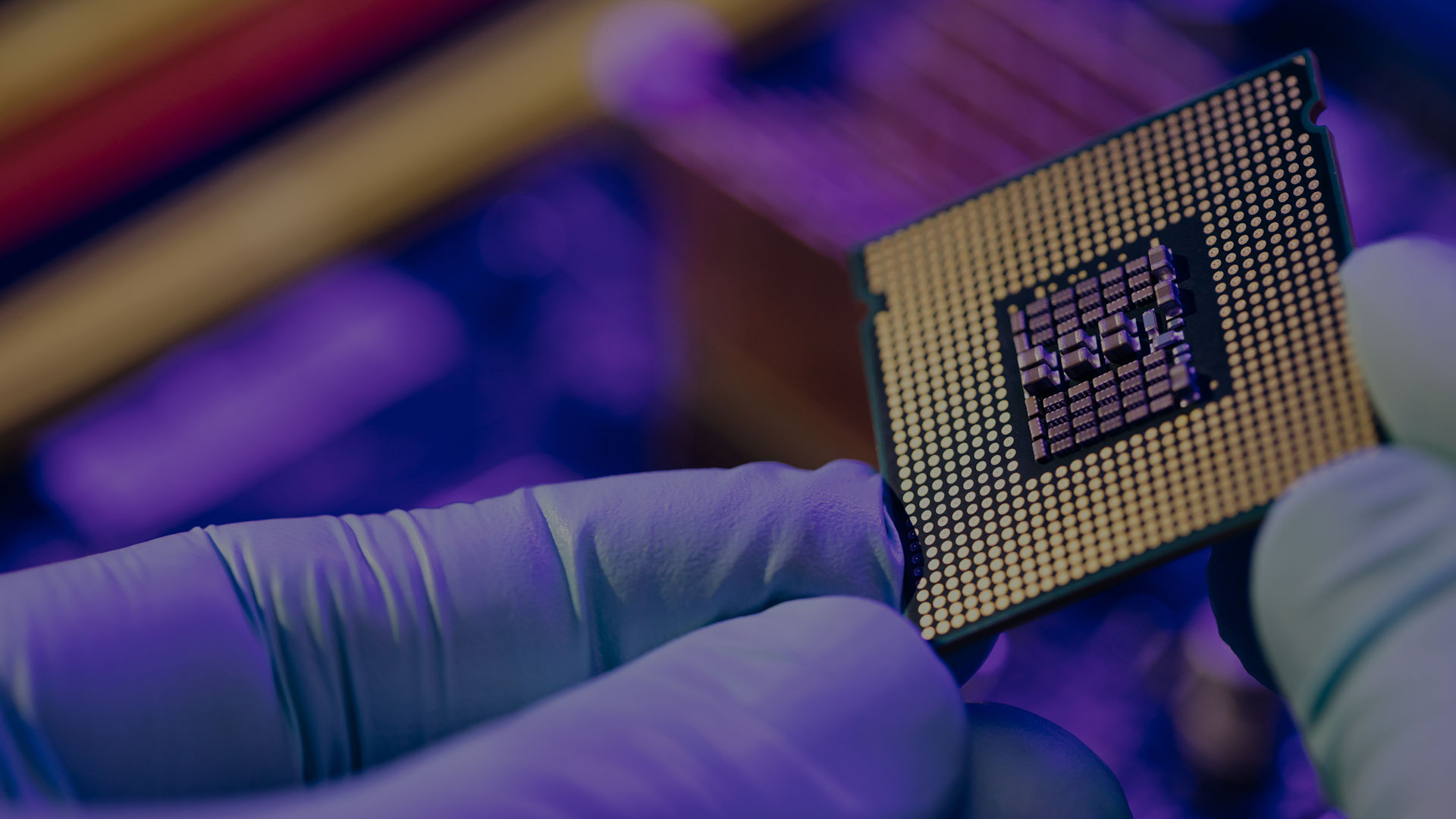
Groundbreaking Innovations
Birck Nanotechnology Center supports a variety of Purdue-affiliated centers doing groundbreaking nanoscale research.
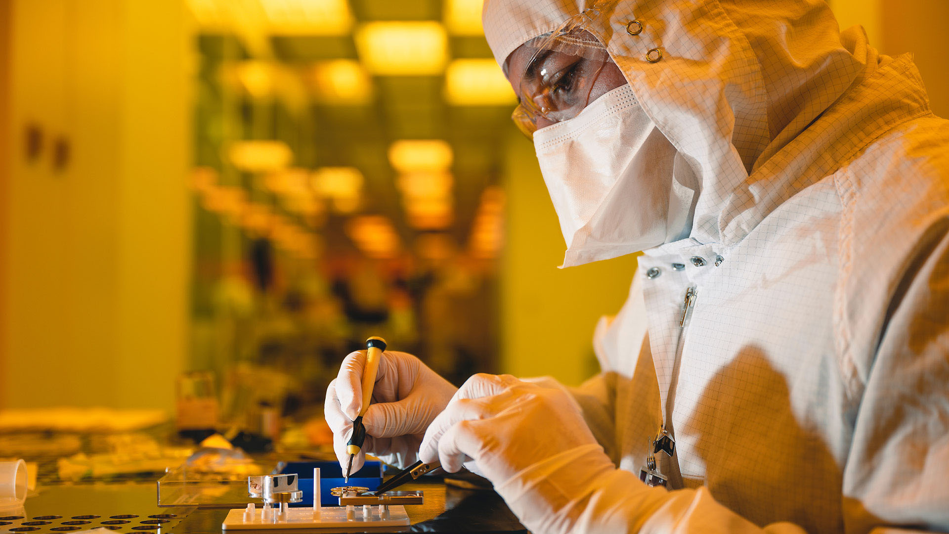
Trailblazing research at Birck
Birck is home to 300 resident students, faculty, and staff who have access to all shared labs. Researchers from six academic colleges are helping to develop a local high-tech ecosystem in collaboration with Discovery Park District.
Research centers
Purdue-affiliated research centers that partner with Birck and/or leverage Birck facilities.
Silicon Crossroads
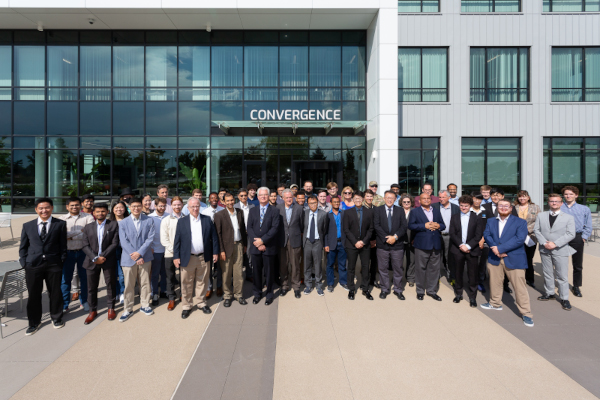
Purdue is a lead academic institution in the 200+ member Silicon Crossroads Microelectronic Commons Hub, led by the Applied Research Institute. Silicon Crossroads is an innovation ecosystem of diverse partners driven to accelerate expansion of America’s microelectronics base by leveraging strong collaborative practices that strategically support innovation, workforce development, and infrastructure needs to achieve domestic microelectronics excellence.
Center for Heterogeneous Integration Research on Packaging (CHIRP)
Heterogeneous integration (HI) of materials and chips into a 2.5D/3D package is increasingly in demand to achieve flexibility of function while achieving low cost through increased manufacturing yield. HI is critical to industries ranging from computing, smartphones to automobiles. CHIRP, which is part of the Semiconductor Research Corporation’s Global Research Collaboration, leverages Birck’s advanced packaging fabrication and metrology capabilities. The center is a collaboration between Purdue and the State University of New York at Binghamton.
Cooling Technologies Research Center (CTRC)
CTRC is a graduated National Science Foundation industry/university cooperative research center that works with Birck. Its focus: high-performance heat removal from compact spaces. CTRC’s research agenda is set by its members, which come from diverse industries. That means beneficial cross-industry interactions are common, and there’s an emphasis on translating findings into new and improved products.
Scalable Asymmetric Lifecycle Engagement (SCALE)
SCALE is the preeminent U.S. program for semiconductor workforce development in the defense sector. Led by Purdue University with support from Purdue’s Discovery Park District, Birck Nanotechnology Center, and the College of Engineering, SCALE is funded by the Department of Defense and managed by NSWC Crane. Addressing the nation’s urgent need for more workers in this space, SCALE provides unique courses, mentoring, internship matching, and targeted research projects in five microelectronics specialties: radiation-hardening, heterogeneous integration/advanced packaging, system-on-chip, embedded system security/trusted artificial intelligence, and radio frequency/optoelectronics.
Center for Secure Microelectronics Ecosystem (CSME)
CSME fosters collaboration among industry, academia and the U.S. government with the aim to ensure a secure supply of materials, semiconductor chips and related tools all the way from the foundry to the packaged system, assuming a zero trust model.
nanoHUB
Birck researchers bring theory and experiment together by working closely with nanoHUB, a National Science Foundation center headquartered at Purdue. With its open and free online platform, nanoHUB provides simulation tools and thousands of other resources, including teaching materials, courses, presentations and workshops.
Purdue Quantum Science and Engineering Institute (PQSEI)
PQSEI focuses on discovering and studying new materials and basic physical quantum systems that can be integrated into future technologies. The institute, which works closely with Birck, encourages interdisciplinary collaboration, leading to creation of industry-friendly quantum devices with enhanced functionality and performance. PQSEI also trains the next generation of quantum scientists and engineers.
Scalable Manufacturing of Aware & Responsive Thin Films (SMART)
Purdue University’s SMART Films Consortium brings interdisciplinary researchers together with industry leaders to address a unifying question: How can Internet of Things (IoT) sensor technology become so affordable it can be produced at mass volumes and deployed over large areas? SMART believes the solution to this challenge is hybrid printed IoT devices, with both silicon and non-silicon sensors.

Atalla Institute for Advanced System Integration and Packaging (ASIP)
Established in October 2023, ASIP puts a new focus on advanced system architecture, design, modeling, fabrication, thermal solutions, metrology, reliability, and sustainability capabilities at Purdue. Chip packaging ensures the functionality and reliability of a system as multiple chips are connected electrically. Such sophisticated packaging enables complex functionality while reducing cost. ASIP is a collaboration among Purdue, Cadence Design Systems, Semiconductor Research Corporation, imec, and Japan’s Osaka University.
Purdue and Semiconductors
Supported by the Birck Nanotechnology Center, Purdue is well positioned to conduct the research and training necessary to boost the U.S. footprint in semiconductors.