
August 26, 2019
Sticker makes nanoscale light manipulation easier to manufacture
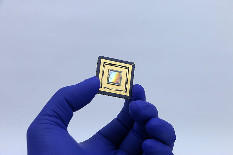
Researchers have given sensors the ability to manipulate light better, thanks to a sticker in the center of this device. (Purdue University image/Bongjoong Kim)
WEST LAFAYETTE, Ind. — Human pathogens, such as HIV and viruses causing respiratory tract infection, have molecular fingerprints that are difficult to distinguish. To better detect these pathogens, sensors in diagnostic tools need to manipulate light on a nanoscale.
But there isn’t a good way to manufacture these light manipulation devices without damaging the sensors. Purdue University engineers have a solution: Stickers.
In a paper published in Nano Letters, the team integrated light manipulation devices called 3D plasmonic nanoarrays onto peelable films that can stick to any surface. They tested the sticker-nanoarray’s capabilities on the lenses of sensors, which make up conventional imaging systems.
The Air Force Research Laboratory supported the work and validated the sticker’s performance and properties.
“Unlike any existing approaches, the entire process occurs in distilled water at room temperature without the chemical, thermal or mechanical treatments that can damage sensitive surfaces, such as a sensor lens,” said Chi Hwan Lee, an assistant professor of biomedical engineering and mechanical engineering at Purdue.
To turn the nanoarrays into a sticker, the researchers built them into a film on a silicon wafer. When submerged in distilled water, the film peels cleanly from the wafer, allowing the wafer to be reused. The film can then stick to the desired surface without damaging it.
“Because this methodology allows 3D plasmonic nanoarrays to physically separate from a donor wafer and transfer over to another surface without defect, it offers a major cost- and time-saving factor in the manufacturing scheme,” Lee said.
The researchers also demonstrated that the process works for various classes of 3D plasmonic nanoarrays in both lateral and vertical configurations, offering more functionality.
Lee’s lab plans to further develop these sticker-nanoarrays for biological sensing applications, such as for protein detection in clinical diagnostics. The lab has already created electronic stickers that serve as bio-patches for drug delivery. They also can enable ordinary objects to wirelessly connect to a network, creating an “Internet of Things.”
The method has been patented via the Purdue Research Foundation Office of Technology Commercialization. This research aligns with Purdue's Giant Leaps celebration, acknowledging the university’s global advancements made in health, longevity and quality of life as part of Purdue’s 150th anniversary. This is one of the four themes of the yearlong celebration’s Ideas Festival, designed to showcase Purdue as an intellectual center solving real-world issues.
Writer: Kayla Wiles, 765-494-2432, wiles5@purdue.edu
Source: Chi Hwan Lee, 765-494-6212, lee2270@purdue.edu
Note to Journalists: For a copy of the paper, please contact Kayla Wiles, Purdue News Service, at wiles5@purdue.edu.
ABSTRACT
Deterministic Nanoassembly of Quasi-Three-Dimensional Plasmonic Nanoarrays with Arbitrary Substrate Materials and Structures
Bongjoong Kim,† Jiyeon Jeon,‡ Yue Zhang,§ Dae Seung Wie,† Jehwan Hwang,‡ Sang Jun Lee,‡ Dennis E. Walker, Jr.,∥ Don C. Abeysinghe,⊥ Augustine Urbas,⊥ Baoxing Xu,*,§ Zahyun Ku,*,⊥ and Chi Hwan Lee*,†,#,∇
† School of Mechanical Engineering, Purdue University, West Lafayette, Indiana, United States
‡ Division of Industrial Metrology, Korea Research Institute of Standards and Science, Daejeon, Korea
- Department of Mechanical and Aerospace Engineering, University of Virginia, Charlottesville, Virginia, United States
∥ Sensors Directorate, Air Force Research Laboratory, Wright-Patterson AFB, United States
⊥Materials and Manufacturing Directorate, Air Force Research Laboratory, Wright-Patterson AFB, United States
#Weldon School of Biomedical Engineering, Purdue University, West Lafayette, Indiana, United States
∇Department of Speech, Language, and Hearing Sciences, Purdue University, West Lafayette, Indiana, United States
DOI: 10.1021/acs.nanolett.9b02598
Guided manipulation of light through periodic nanoarrays of three-dimensional (3D) metal–dielectric patterns provides remarkable opportunities to harness light in a way that cannot be obtained with conventional optics yet its practical implementation remains hindered by a lack of effective methodology. Here we report a novel 3D nanoassembly method that enables deterministic integration of quasi-3D plasmonic nanoarrays with a foreign substrate composed of arbitrary materials and structures. This method is versatile to arrange a variety of types of metal–dielectric composite nanoarrays in lateral and vertical configurations, providing a route to generate heterogeneous material compositions, complex device layouts, and tailored functionalities. Experimental, computational, and theoretical studies reveal the essential design features of this approach and, taken together with implementation of automated equipment, provide a technical guidance for large-scale manufacturability. Pilot assembly of specifically engineered quasi-3D plasmonic nanoarrays with a model hybrid pixel detector for deterministic enhancement of the detection performances demonstrates the utility of this method.
