
| RELATED INFO |
| • Discovery Park |
| • Birck Nanotechnology Center |
| • Purdue Campaign News Page |
| • Purdue Home Page |
October 8, 2005
Purdue's Birck nanotech building now open for business
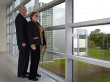
WEST LAFAYETTE, Ind. – Purdue's Birck Nanotechnology Center, considered the best university facility of its kind in the nation, was dedicated during a ceremony Saturday (Oct. 8).
|
"This center has a legitimate claim of being the best academic nanotech facility in the country," Purdue President Martin C. Jischke said.
The Birck Center has been operating since Discovery Park was formed in 2001, but researchers in the center have been using existing laboratories and equipment in campus facilities. The center has already been successful in attracting funding and top faculty, said Alan H. Rebar, interim executive director of Discovery Park.
"We have two national centers located within the center, one funded by the National Science Foundation and the other funded by NASA," Rebar said.
The building was completed in September after construction began in 2003. It will take about a year for scientists and engineers to move all of their equipment into the specialized laboratories in the new center.
|
"While the Birck Center has already been very successful, attracting $38 million in funding and resulting in new opportunities and research projects, there is still more to come," said Provost Sally Mason. "The pace of activity is ramping up for Discovery Park in general, but a big operation like this isn't something that reaches its full potential overnight. We expect it to be bigger and better and continue to grow."
The $58 million center, a two-floor, 187,000-square-foot facility, involves about 260 faculty and staff members and graduate students from 25 schools and departments across the university. A third level houses air filtration equipment.
"The philosophy that we adopted in this center is that we would provide a facility and equipment that are otherwise very difficult for individual faculty members to get on their own," said Richard Schwartz, the center's co-director and a professor of electrical and computer engineering. "This specialized equipment, and being able to work with larger interdisciplinary groups of researchers, is what attracts people to the center.
"One of the really unusual aspects of the center is that all of the lab space and all of the equipment is in the shared mode. That means every member of the center has access to any of the equipment."
The center contains specialized labs designed to control conditions such as vibration, noise, temperature, humidity and electromagnetic interference from radio waves and other sources.
"In particular, the vibration and temperature control are world class in certain laboratories," said James A. Cooper Jr., co-director of the center and a professor of electrical and computer engineering.
The center's designers from HDR Inc., a worldwide architectural-engineering firm headquartered in Omaha, Neb., also designed the Advanced Measurement Laboratory at the National Institute of Standards and Technology, in Gaithersburg, Md., which is among the most advanced measurement facilities in the world.
|
Two labs in the Birck building have floors consisting of thick concrete slabs that float on air-filled shock absorbers for ultra-fine vibration control. The rooms also are surrounded by heavily insulated walls like those of walk-in freezers. Vibration and temperature must be carefully controlled because researchers will be working on the scale of individual atoms. The slightest jarring or expansion from heat would foul up experiments.
"You can keep the air in here stable to plus or minus one-tenth of a degree Celsius," said George Adams, the center's research development manager and an adjunct associate professor of electrical and computer engineering. "We call them the high-accuracy rooms. In these labs we will use scanning probe microscopy and other techniques to examine the structure of materials nearly on an atom-by-atom basis. In order to study specimens on such tiny scales, you have to be able to hold them extremely still, and you also have to control the temperature.
"If I pick up a pencil and hold it in my hand, the warmth from my fingers makes it about a thousand atoms longer because of expansion, so if you want to look at a particular atom, it moves out of your field of view."
Another sophisticated feature of the building is its large suite of "clean rooms," 25,000 square feet of space containing a series of labs that are rated progressively higher based on the number of particles in each cubic foot of air.
|
"It is an awesome building," Schwartz said. "The center is definitely a draw to Purdue. It is helping us recruit top faculty and students in nanotechnology areas."
The lowest-rated lab is still about 100 times cleaner than the average office and contains less than a thousand particles the size of a micron, or millionths of a meter, per cubic foot of air. Another lab will be 10 times cleaner, with about 100 particles per cubic foot of air, and yet another lab will be 10 times cleaner still, with about 10 particles per cubic foot of air.
"To give you some sense of comparison, my office probably has at least 100,000 micron-size particles per cubic foot of air," Schwartz said. "If I were a smoker, we'd be talking millions of particles."
Each of the clean rooms has a separate entryway, inside which researchers don special gowns, or "bunny suits," to prevent them from contaminating the labs.
"These are collectively called the nanofabrication clean room, which will be used to make electronic devices similar to the transistors and circuits in computer chips," Schwartz said. "Clean air is constantly blown into the rooms and then recirculated through filters to keep chasing out the dirt.
"Then we have an adjacent bio-clean room, where we work in a totally germ-free environment, which is important for bio-nano research involving biological molecules and organisms."
In bio-nano research, scientists and engineers are marrying biological molecules, such as proteins and DNA, with electronic devices. The research promises to make possible a new class of portable detectors for a range of applications, such as sensors for quickly testing food for bacterial contamination and sampling the air for biological and chemical warfare agents, as well as advanced medical diagnostic devices for analyzing the blood and bodily fluids.
|
The bio-clean room must be sterile as well as free of particles, requiring a different type of air handling and design.
"If you are working with proteins or DNA, for example, you don't want your work contaminated by extraneous molecules," Schwartz said. "You don't want rogue colonies of viruses or bacteria in there that might interfere with a particular organism that you are trying to study."
The lab is isolated from various pieces of equipment, including pumps and motors, which emit contaminants such as oil particles and gases.
"One of the problems biologists would face in the fabrication room is that normal operation of equipment and machinery tends to put oil vapors into the air," Schwartz said. "So, from a biological point of view, this air is polluted with hydrocarbon vapors and oil vapors. These are not particles, so they can't be removed with filters."
Schwartz said one design feature makes the Birck Center truly unique.
"The biological clean room and the nanofabrication clean room share a common boundary, and we can move materials back and forth between both labs," he said. "Nobody has done that before."
Researchers from both labs will be able to work together on the same experiments by using "glove boxes" common to both labs. A researcher in the bio-clean room will reach into the glove box from one side, and a researcher in the nanofabrication room will reach in from the other side. The facility is believed to be the only laboratory in the world that will enable researchers from fabrication and bio-clean rooms to work together on experiments, Adams said.
|
Numerous companies and organizations have expressed interest in using facilities in the center.
"Many companies contact us, not only about the Birck Center but also about the recently completed Bindley Bioscience Center and other Discovery Park facilities, because it will take a combination of experts from more than one center working together to solve a particular problem," Adams said. "That's why the Discovery Park concept is so powerful.
"Real-world problems involve more than one discipline. A device may contain electronics, plastic polymers, mechanical components, biological molecules and so on. You also need to educate people about new technologies, which can be handled through the Discovery Learning Center, and you have to figure out how to get new technologies into real products, which is the job of the Burton D. Morgan Center for Entrepreneurship."
The two existing national centers already housed at Birck are the NASA Institute for Nanoelectronics and Computing, directed by Supriyo Datta, the Thomas Duncan Distinguished Professor of Electrical and Computer Engineering, and the NSF Network for Computational Nanotechnology, directed by Mark Lundstrom, Purdue's Scifres Distinguished Professor of Electrical and Computer Engineering.
Having the completed building will boost activities in the nanotech center.
"By opening up the new laboratories and research spaces, we are going to be able to do experiments, fabricate devices and materials, make measurements, and so on, that we couldn't do before," Adams said. "Also, because we now have a place to congregate, we are going to be able to bring all these people together – faculty, students, staff and visitors – which we think will stimulate the intellectual environment and speed up the process of coming up with new ideas."
The center contains 12 conference rooms, 45 faculty offices and 15 student offices.
"We've already been working together and holding seminars, but research has been going on in about 23 labs across campus, so it's been scattered all over," Schwartz said. "This will allow us to bring people together much more easily and provide better access to equipment.
"We have enough space for 150 graduate students, and we already have requests that exceed that, so we've arranged for the Bindley Bioscience Center to house 20 of our graduate students."
Bindley is connected to the east side of the Birck Center via a second-floor walkway.
"We've co-designed the buildings to make it easier for people in both centers to work together," Schwartz said. "We did this partly because we think that some of the really early payoffs in nanotechnology will be in the nano-bio area, which will involve both engineering and biological sciences."
One example of such work is research led by Rashid Bashir, a professor of electrical and computer engineering, aimed at creating devices called "biochip" detectors that combine proteins and other biological molecules with electronic components.
To properly design the clean rooms, Purdue enlisted the help of experts from Delphi Electronics & Safety and Eli Lilly and Co.
Underscoring the building's unusual design is the fact that architects who specialize in nanotechnology facilities will hold a national conference at the center next February.
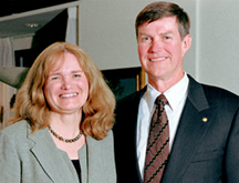
The Birck Center is named for Michael and Katherine (Kay) Birck of Hinsdale, Ill. The Bircks donated $30 million for the building. He is a Purdue alumnus, a member of the Purdue Board of Trustees and chairman of Tellabs Inc. Kay Birck, a Terre Haute, Ind., native, recently retired as head of nursing at Women's Healthcare of Hinsdale.
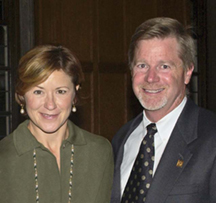
Purdue alumni Donald and Carol Scifres also donated $10 million to the center, and alumni William B. and Mary Jane Elmore provided $2 million toward the center's William and Mary Jane Elmore Advanced Wireless Concept Validation Laboratory.
The dedication is part of a two-week celebration leading up to Purdue's Oct. 15 Homecoming. Events focus on ways Purdue is improving education and helping the state of Indiana as part of the university's strategic plan and $1.5 billion fund-raising campaign.
Writer: Emil Venere, (765) 494-4709, venere@purdue.edu
Sources: Martin Jischke, (765) 494-9708
Alan Rebar, (765) 496-6625, rebar@purdue.edu
Sally Mason, (765) 494-9709, sfmason@purdue.edu
James A. Cooper, (765) 494-3514, cooperj@purdue.edu
George B. Adams, (765) 494-2698, gba@purdue.edu
Richard Schwartz, (765)494-0619, schwartz@purdue.edu
Purdue News Service: (765) 494-2096; purduenews@purdue.edu
PHOTO CAPTION:
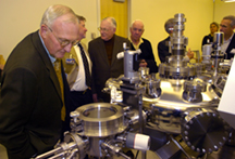
Michael J. Birck, at left, looks at a mass spectrometer during a
lab tour at the new $60 million Birck Nanotechnology Center in
Purdue's Discovery Park. Behind him are alumnus William B. Elmore,
astronaut and alumnus Neil Armstrong, and former Purdue trustee
Bob F. Jessie. The center was dedicated today (Saturday, Oct. 8)
before a crowd of about 250 people. The center is named for
Michael and Katherine (Kay) Birck, who donated $30 million for the
facility. William and Mary Jane Elmore donated $2 million toward
the center's Elmore Advanced Wireless Concept Validation
Laboratory. (Purdue News Service photo/David Umberger)
PHOTO CAPTION:
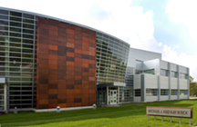
Purdue's Birck Nanotechnology Center, considered among the best university facilities designed specifically for research in nanotechnology, will be dedicated during an Oct. 8 ceremony. The $58 million center, a two-floor, 187,000-square-foot facility, involves about 260 faculty and staff members and graduate students from 25 schools and departments across the university. (Purdue News Service photo/David Umberger)
A publication-quality photograph is available at https://www.purdue.edu/uns/uns/images/+2005/birck-nanocenter-ext.jpg
PHOTO CAPTION:
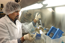
Samir Iqbal, a doctoral student in the School of Electrical and Computer Engineering, works under a laboratory hood to transfer a small amount of DNA solution to electronic chips. DNA attaches to gold molecules on such "biochips" in a technology that offers promise for creating devices for detecting bacteria and other substances by combining proteins, DNA and other biological molecules with electronic components. Such chips might be used to detect cancer cells and cancer-related proteins. (Purdue News Service photo/David Umberger)
A publication-quality photograph is available at https://www.purdue.edu/uns/uns/images/+2005/bashir-lab-chip.jpg
To the News Service home page